- 您现在的位置:买卖IC网 > Sheet目录2008 > MAX11616EEE+T (Maxim Integrated Products)IC ADC SERIAL 12BIT 12CH 16-QSOP
MAX11612–MAX11617
Low-Power, 4-/8-/12-Channel, I2C,
12-Bit ADCs in Ultra-Small Packages
15
Maxim Integrated
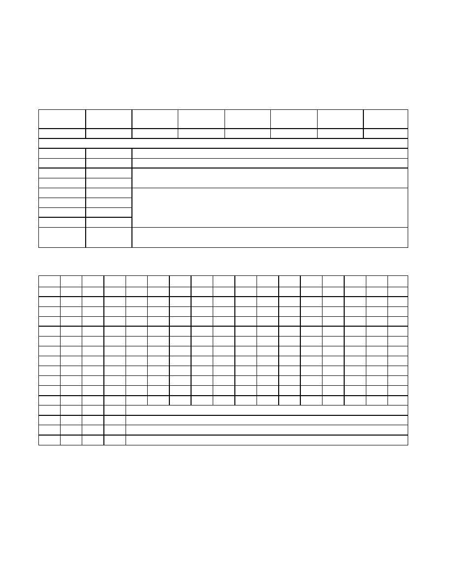
BIT 7
(MSB)
BIT 6
BIT 5
BIT 4
BIT 3
BIT 2
BIT 1
BIT 0
(LSB)
REG
SCAN1
SCAN0
CS3
CS2
CS1
CS0
SGL/DIF
BIT
NAME
DESCRIPTION
7
REG
Register bit. 1 = setup byte (see Table 1), 0 = configuration byte.
6
SCAN1
5
SCAN0
Scan select bits. Two bits select the scanning configuration (Table 5). Default to 00 at power-up.
4
CS3
3
CS2
2
CS1
1
CS0
Channel select bits. Four bits select which analog input channels are to be used for conversion
(Tables 3 and 4). Default to 0000 at power-up. For the MAX11612/MAX11613, CS3 and CS2 are
internally set to 0. For the MAX11614/MAX11615, CS3 is internally set to 0.
0
SGL/DIF
1 = single-ended, 0 = differential (Tables 3 and 4). Defaults to 1 at power-up. See the Single-
Ended/Differential Input section.
Table 2. Configuration Byte Format
CS3
1
CS2
1
CS1
CS0
AIN0
AIN1
AIN2
AIN3
2
AIN4
AIN5
AIN6
AIN7
AIN8
AIN9
AIN10 AIN11
2
GND
0
000
+
-
0
001
+
-
0
010
+
-
0
011
+
-
0
100
+
-
0
101
+
-
0
110
+
-
0
111
+
-
1
000
+
-
1
001
+-
1
010
+-
1
011
+
-
1
0
RESERVED
1
0
1
RESERVED
1
0
RESERVED
1
RESERVED
1For the MAX11612/MAX11613, CS3 and CS2 are internally set to 0. For the MAX11614/MAX11615, CS3 is internally set to 0.
2When SEL1 = 1, a single-ended read of AIN3/REF (MAX11612/MAX11613) or AIN11/REF (MAX11616/MAX11617) is ignored; scan
stops at AIN2 or AIN10. This does not apply to the MAX11614/MAX11615 as each provides separate pins for AIN7 and REF.
Table 3. Channel Selection in Single-Ended Mode (SGL/
DIF = 1)
发布紧急采购,3分钟左右您将得到回复。
相关PDF资料
MAX1162AEUB+T
IC ADC 16BIT 200KSPS 10-MSOP
MAX11637EEE+T
IC ADC 12BIT 8CH 16QSOP
MAX11643EEG+T
IC ADC 8BIT 8CH 24QSOP
MAX11645EUA+T
IC ADC 12BIT I2C/SRL 1CH 8UMAX
MAX11647EUA+T
IC ADC 10BIT I2C 94.4KSPS 8UMAX
MAX1166BEUP+
IC ADC 16BIT 165KSPS 20-TSSOP
MAX1168BCEG+
IC ADC 16BIT 200KSPS 24-QSOP
MAX1183ECM+TD
IC ADC 10BIT 40MSPS DL 48-TQFP
相关代理商/技术参数
MAX11616EVKIT+
功能描述:数据转换 IC 开发工具 MAX11616 Eval Kit
RoHS:否 制造商:Texas Instruments 产品:Demonstration Kits 类型:ADC 工具用于评估:ADS130E08 接口类型:SPI 工作电源电压:- 6 V to + 6 V
MAX11616EVSYS+
功能描述:数据转换 IC 开发工具 MAX11616 Eval Kit
RoHS:否 制造商:Texas Instruments 产品:Demonstration Kits 类型:ADC 工具用于评估:ADS130E08 接口类型:SPI 工作电源电压:- 6 V to + 6 V
MAX11617
制造商:MAXIM 制造商全称:Maxim Integrated Products 功能描述:2.7V to 3.6V and 4.5V to 5.5V, Low-Power, 4-/8-/12-Channel, 2-Wire Serial, 12-Bit ADCs
MAX11617DB+
功能描述:模数转换器 - ADC Integrated Circuits (ICs) Data Acquisition - Analog to Digital Converters - IC ADC 12BIT 12CH LP 16QSOP RoHS:否 制造商:Texas Instruments 通道数量:2 结构:Sigma-Delta 转换速率:125 SPs to 8 KSPs 分辨率:24 bit 输入类型:Differential 信噪比:107 dB 接口类型:SPI 工作电源电压:1.7 V to 3.6 V, 2.7 V to 5.25 V 最大工作温度:+ 85 C 安装风格:SMD/SMT 封装 / 箱体:VQFN-32
MAX11617EEE+
功能描述:模数转换器 - ADC 12-Bit 12Ch 94.4ksps 3.6V Precision ADC
RoHS:否 制造商:Texas Instruments 通道数量:2 结构:Sigma-Delta 转换速率:125 SPs to 8 KSPs 分辨率:24 bit 输入类型:Differential 信噪比:107 dB 接口类型:SPI 工作电源电压:1.7 V to 3.6 V, 2.7 V to 5.25 V 最大工作温度:+ 85 C 安装风格:SMD/SMT 封装 / 箱体:VQFN-32
MAX11617EEE+T
功能描述:模数转换器 - ADC 12-Bit 12Ch 94.4ksps 3.6V Precision ADC
RoHS:否 制造商:Texas Instruments 通道数量:2 结构:Sigma-Delta 转换速率:125 SPs to 8 KSPs 分辨率:24 bit 输入类型:Differential 信噪比:107 dB 接口类型:SPI 工作电源电压:1.7 V to 3.6 V, 2.7 V to 5.25 V 最大工作温度:+ 85 C 安装风格:SMD/SMT 封装 / 箱体:VQFN-32
MAX11617EVKIT+
功能描述:数据转换 IC 开发工具 MAX11617 Eval Kit RoHS:否 制造商:Texas Instruments 产品:Demonstration Kits 类型:ADC 工具用于评估:ADS130E08 接口类型:SPI 工作电源电压:- 6 V to + 6 V
MAX11617EVSYS+
功能描述:数据转换 IC 开发工具 MAX11617 Eval Kit
RoHS:否 制造商:Texas Instruments 产品:Demonstration Kits 类型:ADC 工具用于评估:ADS130E08 接口类型:SPI 工作电源电压:- 6 V to + 6 V